Everything you want to do with S parameters in one place
ADK is a comprehensive set of SI utility tools to simplify many commonly encountered SI tasks into a single mouse click. ADK has been used daily for many years in major hardware companies. With ADK, new graduates can be trained to perform the tasks of middle-level SI engineers within a day. Among the 25+ SI Apps are
- Fill in DC and correct passivity, reciprocity and causality errors in Touchstone files,
- Convert S parameters into TDR/TDT waveforms,
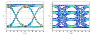
- Compute optimized TX tap coefficients, run channel simulation and plot eye diagrams,
- Convert S parameters into tabular RLGC models,
- Convert S parameters into equivalent SPICE models,
- Combine multiple .snp files,
- Channel Operating Margin (COM) for IEEE 802.3
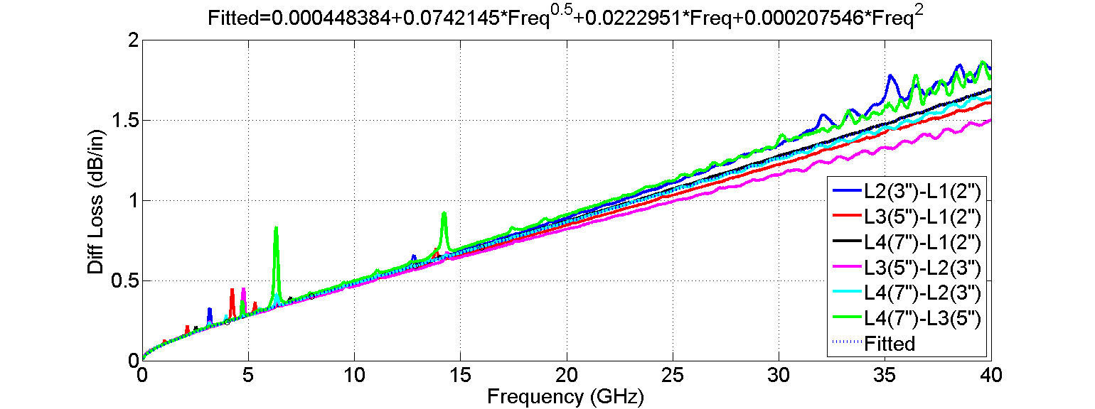
- Delta L 4.0 with curvefitted equation and more
- Many templates to extract DK, DF and roughness
- Compliance testing (IL, RL, power-sum crosstalk, ICR, ICN, ccICN), 2D field solver, S-param viewer and more.
See Presentation for more details.
Example 1
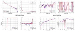
ADK’s proprietary algorithm corrects casuality error and noise of measurement data where popular vector-fitting-based programs fail to do.
Example 2
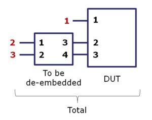
Crucial for active-device verification, ADK is the only tool that can de-embed arbitrary N ports from M ports.
Example 3
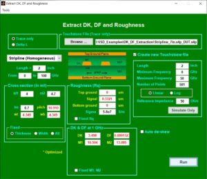
ADK’s interactive GUI makes DK/DF/SR extraction a breeze.
Example 4
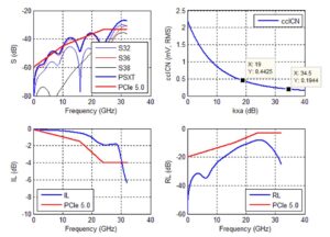
Compliance testing for PCIe 5.0 is just one click away:
Example 5
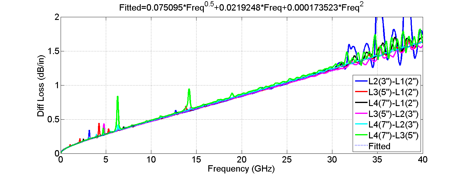
Delta-L is used to compute PCB loss from multiple Touchstone files of different trace length. Curvefitted equation is provided. ADK’s unique automated de-skew feature helps reduce variation of PCB loss.
Without de-skew:
With de-skew:
Example 6
Going from S parameters to optimized TX FFE and RX CTLE and DFE coefficients and eye diagrams in NRZ or PAM-4 is only one mouse click away.
